
OLED and QLED Background Capability to Meet Customer Demands
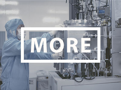
In-house device characterization
- Sputtering
- UV lithographic mask aligner
- VTE and plasma enhanced CVD system
- Light distribution/integrating sphere

OLED lifetime killer identification
- Customized chamber to examine the impurities
- Long-term VTE runs mimicking mass
- OLED lifetime measurement
- HPLC/TG-DTA/TOF-SIMS, etc.
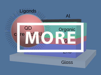
Validation of QLEDs and perovskites
- Size dispersion and film quality control
- Cd-free QLED evaluation
- EQE and lifetime reproducibility
- Cross-sectional TEM, SEM-EDX, etc.
Toward Soft Electronics and XR Applications
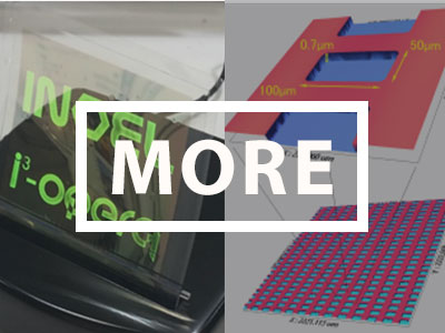
Barrier and micro-structuring
- Low temperature (60℃) CVD
- Thin-film encapsulation
- Stepper lithography and dry-etching
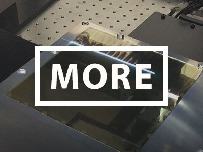 Laser lift-off for flexible devices
- Wearable device fabrication
- Verification of functional materials
- Proof-of-Concept for sensor applications
 Organic-on-Si
- 3D wiring and packaging on Si wafer
- MEMS structuring
- Proof-of-Concept for micro-OLED or organic-CMOS architectures